DC/DC voltage converters - step-down, step-up, and isolated - open hardware construction, Kicad schematics and PCB provided
For many purposes I needed step-down or step-up DC/DC regulators as well as isolated DC/DC (up/down/dual output) regulators. Since the Chinese PCB manufacturers offer 10 boards of the dimension 5x5cm and 5x10cm, I designed them using these dimensions, respectively. All constructions mentioned here are open hardware and GPLv3 licensed.Step-down DC/DC convertor
The step down is based on LM2575/2576 in TO220-5 and supports both fixed voltage and adjustable version with external voltage divider. For the step-down version, when built for 5V, USB connector footprints are provided as well as resistor dividers for D+ and D- pins defining USB charger are included. I have built one such USB charger into a little box attached to the cable of my laptop power adapter in order to charge my phone without a need to switch my laptop on or to have a separate phone charger (and the hassle with another mains adapter when traveling). Schematics is in PDF and KiCad design is in step down ZIP file.Step-up DC/DC convertor
The step up convertor is based on LM2577 in the adjustable version with external voltage divider. A typical application was to power a 48V PoE switch directly from a 12V lead acid battery, avoiding UPS and mains/48V power adapter. Schematics is in PDF and KiCad design is in step up ZIP file.Isolated DC/DC convertor
The isolated DC/DC convertor (down or up) is based on LM3524N and uses custom wound transformer on fe powder core (although it is not flyback but regular center-tapped transformer, but ferrite would give too high inductance) using 2x22 turns primary for 14V input, about 15 turns secondary for 5-7 V. Schematics is provided in PDF and KiCad design is in ZIP file.How to digitally control output voltage of a DC/DC convertor by a microcontroller software
For simplicity we will confine the discussion to a step down convertor. There are basically three possibilities:1) Implement the whole control of DC/DC switching convertor in the MCU, using its built-in peripherals like timers/counters/PWM generators and ADC or comparator for feedback. I did this in other project for special purposes, where a handy chips like LM2576 would not be sufficient for too high current or so. It is also educationally interesting, but the most laborious approach, it complicates the firmware, maybe a more complicated MCU would be needed etc.
2) The most straightforward is to use a "digitally controlled potentiometer", by a I2C or SPI bus in the voltage feedback divider of the above constructions with standard DC/DC switching controllers. This is conceptually simplest, easy to handle in the MCU firmware, but requires an additional chip like DS1803 or AD8400.
Switching power supply (dc/dc step down) with DAC/PWM voltage-controlled output voltage
3) There is an interesting simpler possibility if your MCU contains a DAC convertor or PWM generator. The DAC typically has too high output impedance so it has to be buffered/amplifier by an op-amp. Alternatively, a PWM modulated signal averaged over a low pass RC filter can be used as a source of the control voltage, if DAC/operational amplifier is not preferred, at the cost of possible less accuracy and some ripple. This amplified DAC / averaged PWM voltage we will denote Vdac and connect it via a resistor R3 to the feedback pin of LM2576. The complete connections of the feedback pin are via R1 to GND, via R2 to Vout, and via R3 to Vdac.In the following text we give a complete derivation of the appropriate formulas for the choice of R1,R2,R3 based on the required voltages. Since the current going into the feedback pin of LM2576 is below 100nA, we will neglect it and solve the resistor network using Kirchhoff's laws. The voltage at the feedback pin is kept constant by the switching regulator (e.g. 1.235V for LM2576) and will be denoted Vfb. One can denote the currents going through the individual resistors i1,i2,i3 and write one current conservation equation i1=i2+i3 and three Ohm's law equations, eliminate the current variables and solve for Vout. After a few lines of high school algebra one obtains for the output voltage the formula
Vout = Vfb(1+R2/R1+R2/R3*(1-Vdac/Vfb))
Obviously, if Vdac is confined to the 0-Vin interval, the highest Vout is obtained for Vdac,max=0 and its value is
Vout,max = Vfb(1+R2*(R1+R3)/(R1*R3))
The minimum Vout,min = Vfb, due to the regulator's operating principle, and this value is achieved at Vdac greater or equal to
Vdac,min >= Vfb * (R1+R3)/R1
The resistor R1 is chosen arbitrarily from the range 1-5kohm (according to the LM2576 datasheet). To obtain the values of R2 and R3, let's suppose we amplified Vdac to the range 0-Vin. Then to achieve Vout regulation over the whole scale we equate Vin=Vdac,min and get from the last non-equality the condition
R3 <= R1 * (Vin/Vfb-1)
Requiring Vout,max = Vin we get
Vin/Vfb - 1 = R2/R3*(R1+R3)/R1
Combining this with a previous inequality we get for R2
R2 >= R3 * (1-Vfb/Vin)
If we take for simplicity the value R2=R3, this condition is automatically fulfilled and the resulting equations will be simplified considerably:
Vout = Vfb*(1+R2/R1+1-Vdac/Vfb) = Vfb*(2+R2/R1)-Vdac
Vout,max = Vfb*(2+R2/R1)
To achieve full scale regulation, we set Vout,max = Vin, and solve for the R2 value
R2 = R1 * (Vin/Vfb-2)
In practice, Vin/Vfb is substantially higher than 2 so this condition can be fulfilled. For this choice of R2 and R3=R2, we finally get the extremely simple equation
Vout = Vin - Vdac
Therefore a full range regulation of Vout between Vfb and Vin can be achieved and Vout is linearly decreasing with the imposed Vdac from the interval 0...Vin-Vfb. For example, if Vin=15V and Vfb=1.235V, Vin/Vfb is approximately 12, so we can conveniently take R2 = R3 = 10 R1.
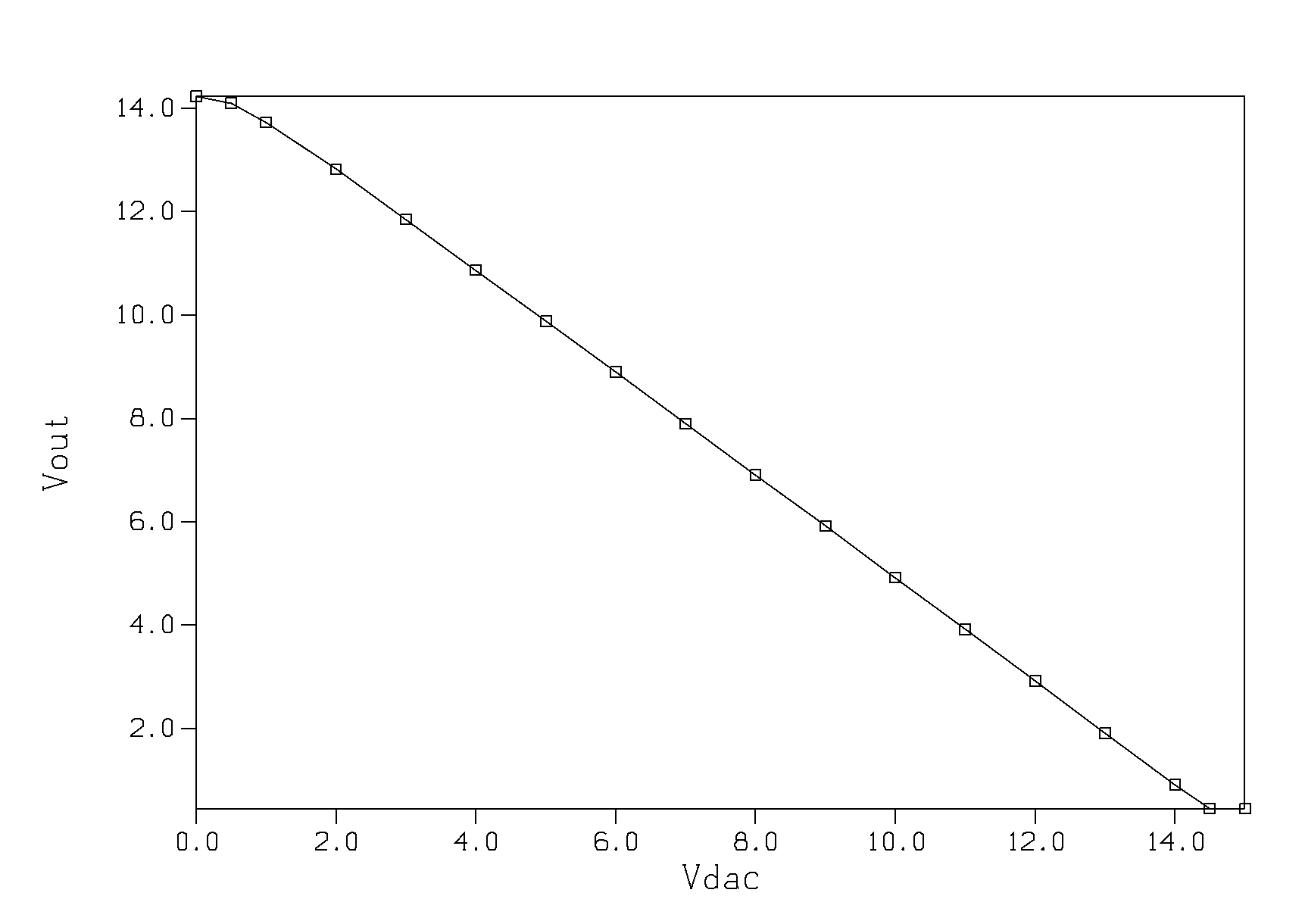
So far the theory, but I have also verified it experimentally, using LM2576, 68uH inductor on iron powder toroid core, 2x 1000uF low ESR capacitors and 1N5822 Schottky diode for the circuit connected according to datasheet, R1=1k, R2=R3=10k. In the figure showing dependence of Vout on Vdac, for constant Vin=15V you can see excellent linearity of the dependence except in the first and last volt of the scale, and small absolute offset about 0.1V.
Calculation of the resistor values for the feedback network of voltage-controlled DC/DC convertor
Let us now analyze the more general case R2 != R3, which can be used if we do not want to amplify Vdac to the 0...Vin range, but leave it in the 0...Vcc range of the MCU employed (check also whether DAC or PWM GPIO PIN can source/sink sufficient current i3 = (Vdac-Vfb)/R3 and select R1 accordingly (within datasheet limits), otherwise some op-amp buffering is needed anyway).We assume R1 is chosen arbitrarily and then determine the two variables R2 and R3 from the condition that Vout should reach Vin for Vdac=0 and it should reach 0 for Vdac=Vcc:
Vin/Vfb = 1 + R2 (1/R1 + 1/R3)
0 = Vfb(1+R2/R1+R2/R3*(1-Vcc/Vfb))
After some algebra the solution of these equations is obtained:
R2/R1 = Vin/Vfb - Vin/Vcc - 1
R3/R1 = Vcc/Vfb - Vcc/Vin - 1
Notice that
R2/R3 = Vin/Vcc
Inserting these values into the Vout formula we get a simple result confirming the linear dependence of Vout on Vdac and covering the whole required output voltage range:
Vout = Vin * (1 - Vdac/Vcc)
Clearly, these results are consistent with the previous special case when inserting Vcc = Vin. The condition that both R2 and R3 have a physically meaningful (positive) value is easily obtained as
1/Vfb > 1/Vin + 1/Vcc
For the 'practical' values obeying Vin >= Vcc > 2*Vfb, it is obviously fulfilled. For example, assuming Vin=15V, Vfb=1.235V, Vcc=5V and R1=1k we get after rounding the resistor values R2 = 8k2 and R3 = 2k7; for Vcc=3.3V then R2 = 6k8 and R3 = 1k5. Notice that Vin above means actually the maximum output voltage, so if that is smaller than the real input voltage, use its value.
This technique was applied for example in an inductor saturation tester.
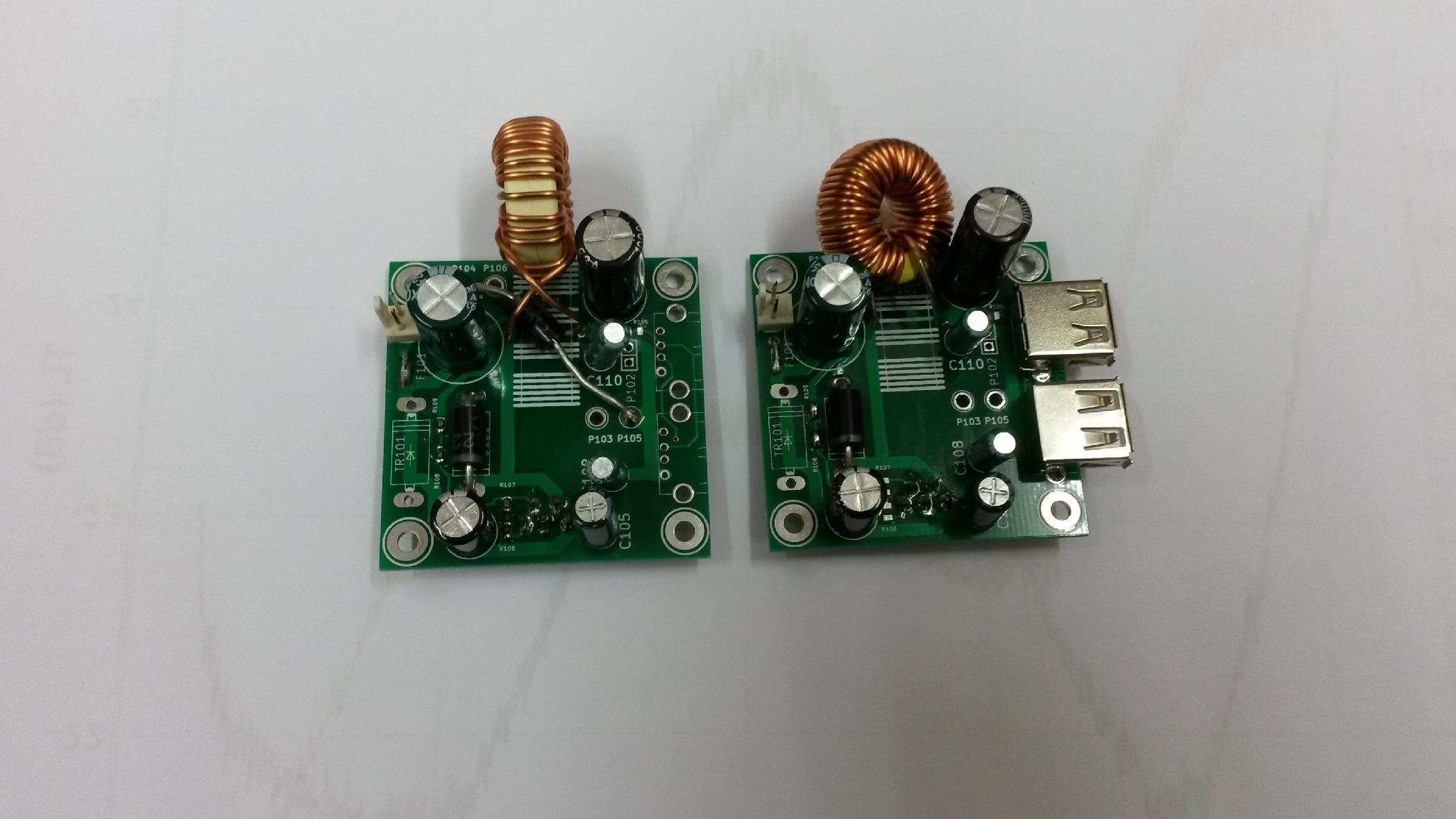
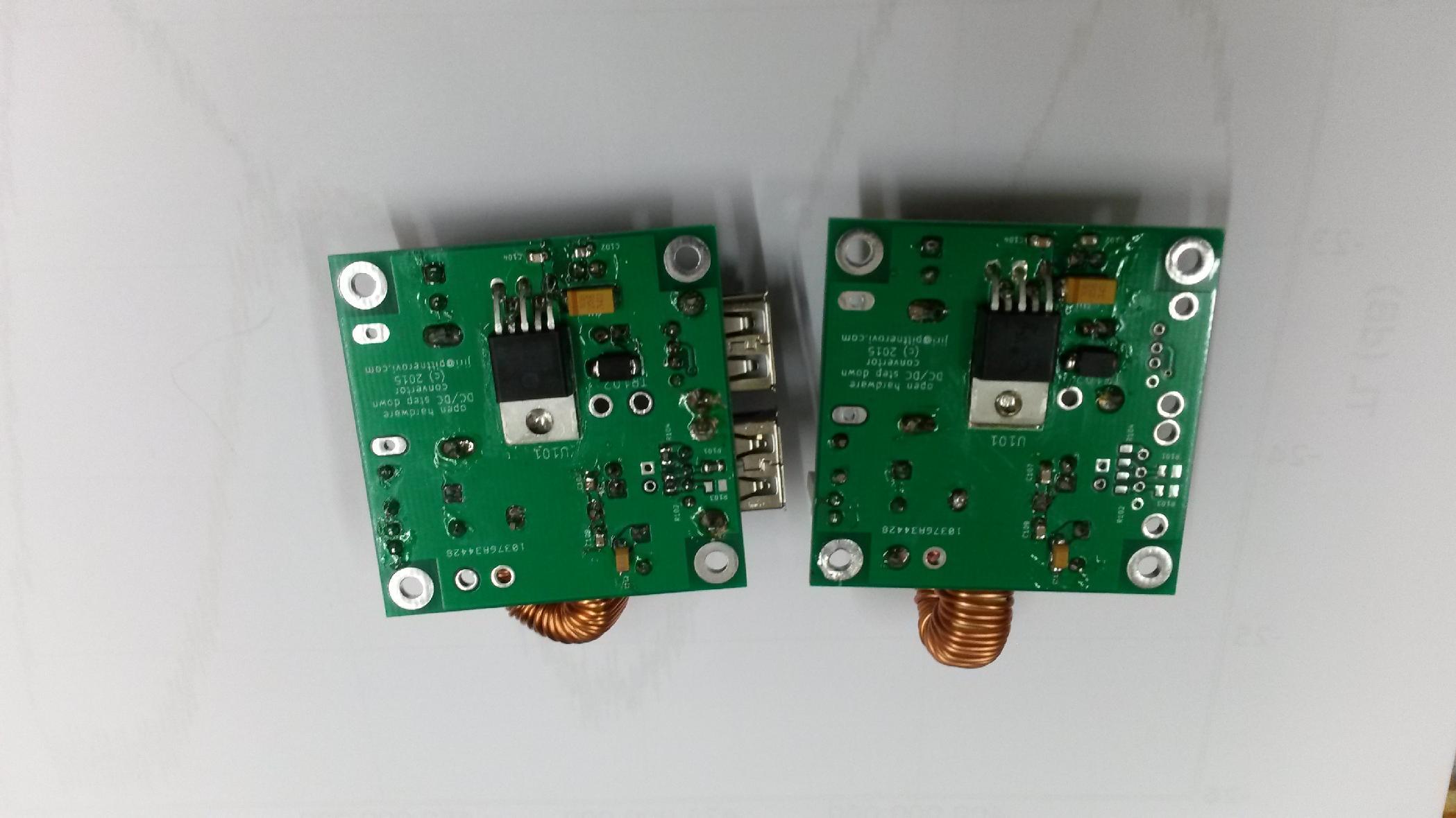
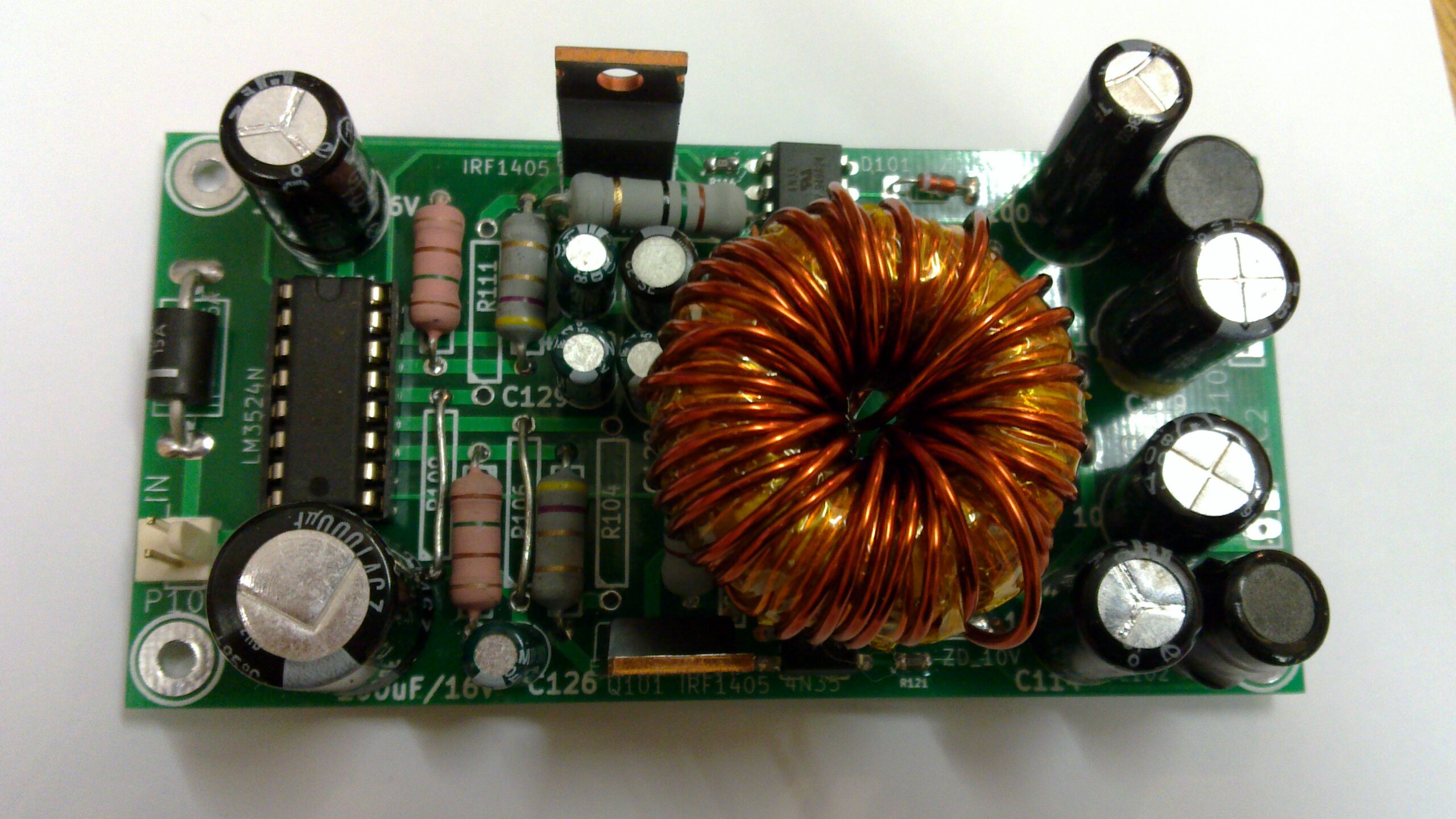
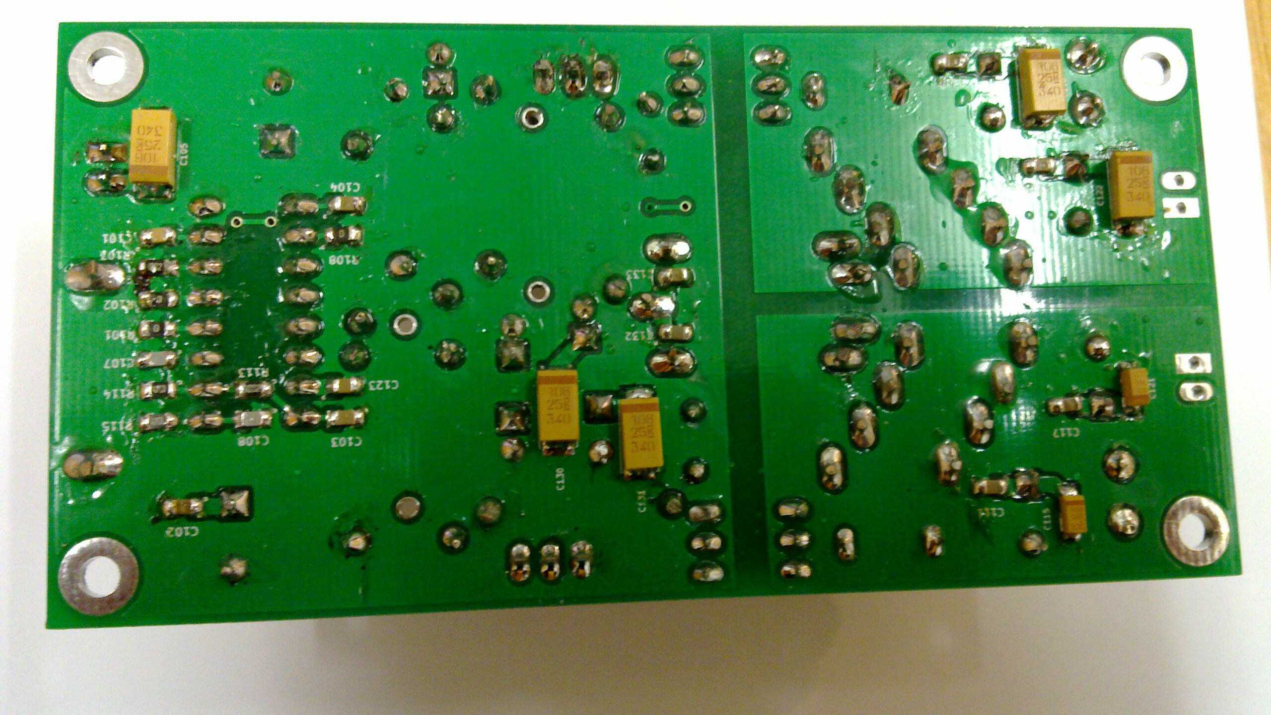
Below are some photos of the pcbs:
Back to my electronics page
Back to my hobby page
Back to my main page
TOP