A simple open hardware electronic ballast for fluorescent lamps
Schematics, KiCad PCB design and Gerber files provided
Why to home-build such an easily commercially available thing as an electronic ballast for fluorescent lamps?Well, the reason is the cost-optimization of the commercial designs, which leads to such a limited lifetime of the device, which barely exceeds the warranty period. After buying and exchanging the 8-th replacement ballast for 6 pieces of 58W fluorescent lamps I have in use, I finally lost my patience and designed and built my own one, which should be more robust.
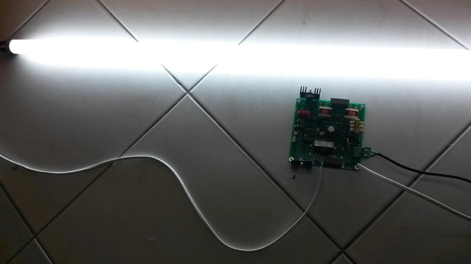
Besides the cost-optimization, another reason for the quick failure of the commercial design is its mechanical form, which should fit into the lamp just above the fluorescent tube. This leads to a horrible thermal design - the ballast is heated by the tube, and the heat it generates from switching losses has limited ways to dissipate. Due to space limitations, there were not even smallest heatsinks on the TO220 transistors in the factory ballast. I decided to give up on the mechanical limitations, so my ballast has to be mounted externally to the lamp, which is inconvenient, but it should be outweighed by its hopefully much longer lifetime. One ballast can drive one or two 58W fluorescent tubes.
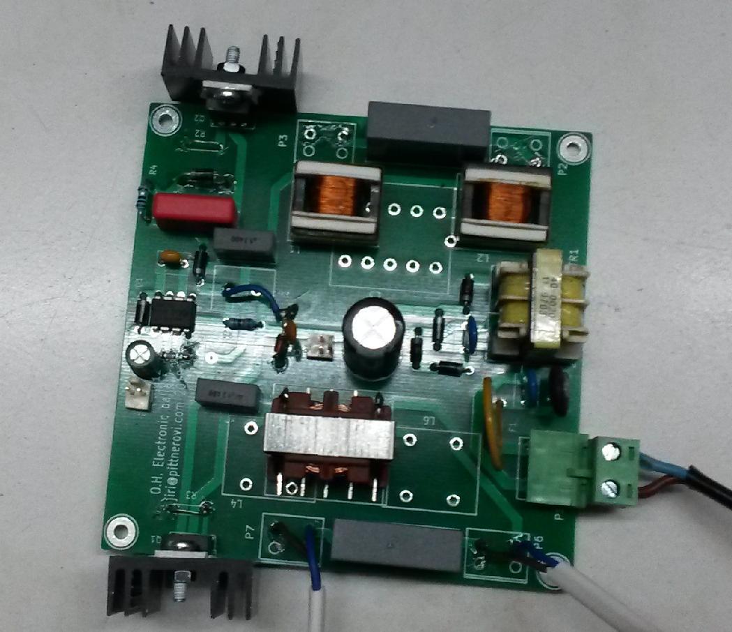
My design basically follows the one by Danyk , with a few small modifications. The schematics is ballast.pdf and here are the complete Open Hardware KiCad design files ballast.zip .
To avoid the heat-generating resistor 33k/5W I employed capacitive voltage drop to power IR2153, from the output of the half-bridge, with a 470k/0.6W resistor for startup. I used 15nF resonance capacitors and slightly different resonance frequency. For the choke serial to the lamp I have two alternatives - home-made 1.6mH choke wound by 0.35mm enameled copper wire on the EF25 ferrite core with a vertically oriented bobbin, or two 0.8mH chokes in series, which were salvaged from the failed commercial ballasts. The choke must have an air gap in the core to prevent saturation - otherwise the device and the lamp will fail badly! The inductance at DC bias should be checked if you build your own choke. Its precise value is not critical, difference of +/- 0.1mH is OK. For lamps of smaller wattage the inductance has to be appropriately higher. The resonance capacitors C11 and C14 must be rated to 1600V DC and their value chosen so that with the choke they resonate at 30-40kHz. The frequency is then set for the IR2153 chip by a suitable choice of R1,R101,C1,C102 (for convenient fine tuning I have placed two capacitors in parallel and two resistors in series); see the datasheet of IR2153 for the choice of their values. The common mode filter choke TR1 is salvaged from a broken PC power supply.
The operation principle is that the lamp is ignited by the high voltage generated on the capacitors C11 (C14 for the second lamp), which resonate in series with the choke, connected through the lamp's filaments. The ignition voltage is around 1000V. Once ignited, the ionized gas column in the lamp effectively shorts the capacitor C11 and the AC current limited by the choke's inductance flows through the lamp. If the lamp fails, typically due to a burned filament, no current can flow and no harm should happen to the ballast. However, note that the ballast is not designed for long-term operation in the mode when it drives a lamp with intact filaments, but which is not ignited. This is typically due to off-resonance of the LC circuit and thus low voltage on C11, below the ignition voltage. The serial LC circuit has then small impedance, large current flows and the transistors become overheated and would fail if this condition persists. Thus when testing the circuit (experimentally optimizing for the best frequency), if the lamp does not ignite instantly, switch it off after 2 seconds. If the transistors would not fail, the filaments could burn as another failure mode. When tuned properly, the lamp should ignite in a fraction of second after power on and transistors should remain almost cold all the time (test it when switched off - connected to mains voltage!).
The device was designed for 230V mains; it operates at substantially lower voltage too, with smaller luminosity, but for 110V mains there could be problems with the ignition, so a redesign using a voltage doubler instead of the bridge rectifier at the input would be needed.
On this picture is the first version of the PCB, where I had to do some modifications (blue wire), however, that above design files and schematics have already been corrected and PCB design respinned.
My Electronics page
My hobby page
My main page with e-mail contact
TOP of my family pages